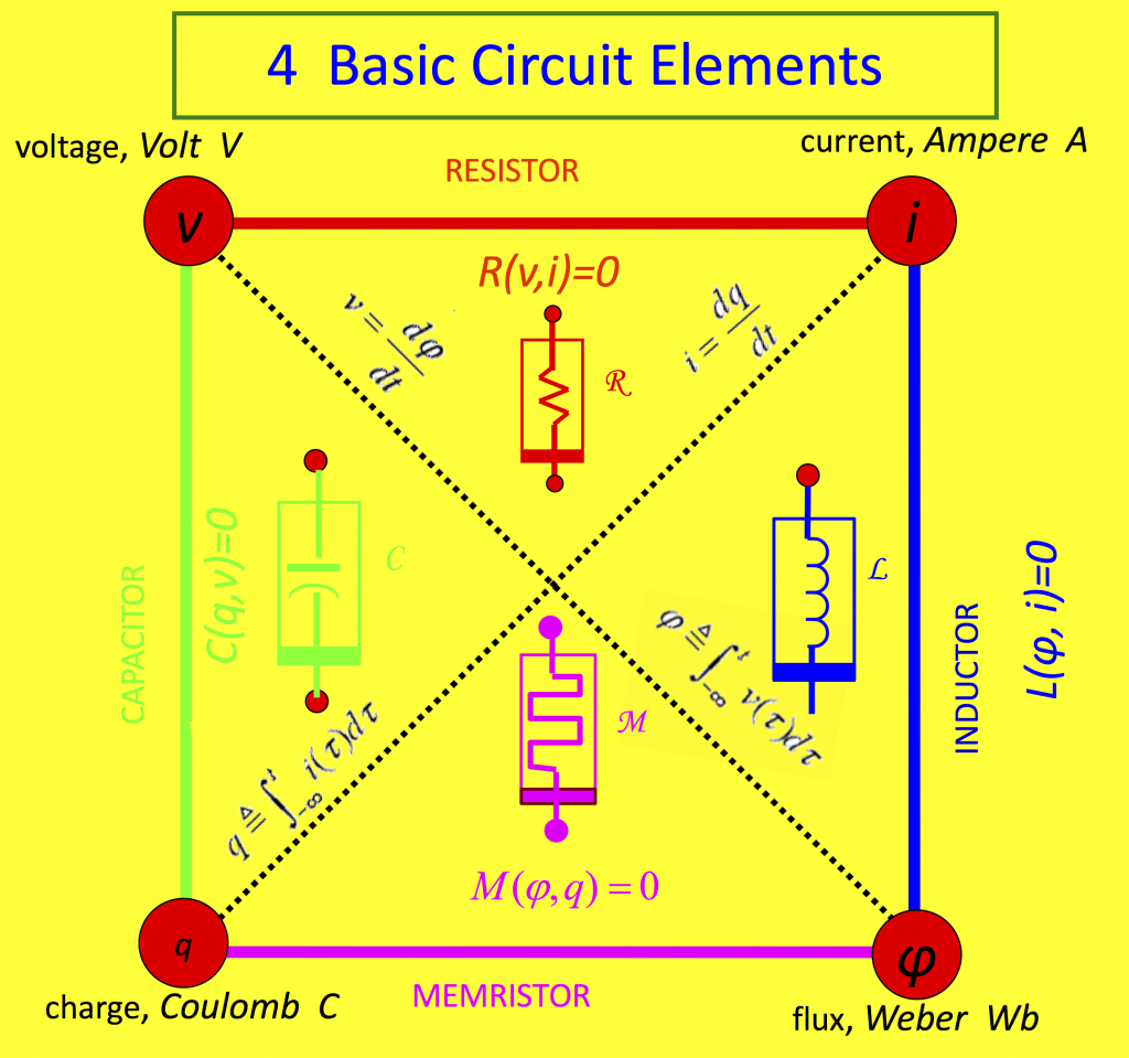
Memristors are two-terminal resistive devices with memory. In general, their nonlinear dynamic behaviour is mathematically modeled by means of a differential algebraic equation (DAE) set, in which an ordinary differential equation (ODE) governs the time evolution of the memory state, while an algebraic relation captures the state- and input-dependent Ohm law. The memristor, an acronym for memory resistor, was theoretically introduced in 1971 by L.O. Chua, whom the Chua Memristor Center (CMC) is dedicated to. The memristor introduced in the 1971 pioneering paper, presently referred to as ideal memristor, is the fourth fundamental two-terminal circuit element, the other three being the resistor, the capacitor, and the inductor, as shown in Fig. 1.
Fig. 1: Basic Circuit Elements
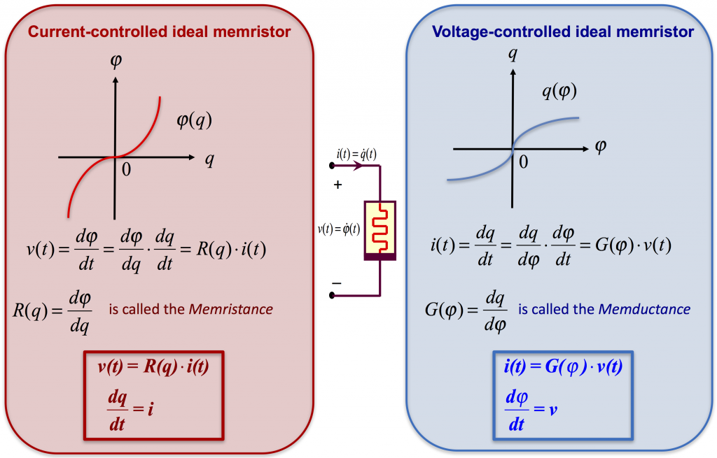
Fig. 2: Ideal Memristor models
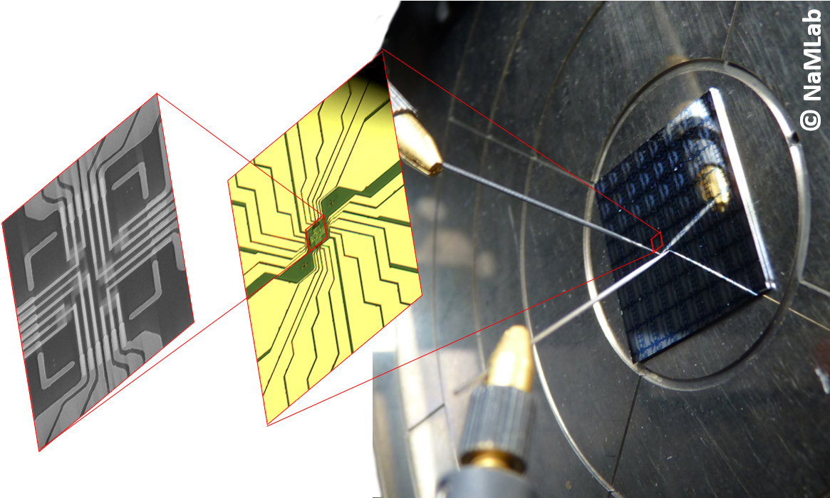
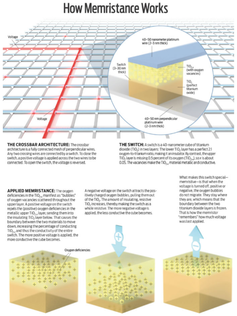
The ideal memristor may be uniquely characterized by a nonlinear relation of the kind f(q,φ)=0 between charge q and flux φ, i.e. between the time integrals of current i and voltage v (the past history of these physical quantities is in fact at the origin for the device memory capability), or equivalently by a simple DAE set, reported in Fig. 2 for both the current and voltage input case. The topic of memristors remained an exclusive research field of theoreticians until the 2008 seminal paper from R.S. Williams and his team of engineers at Hewlett Packard (HP) Labs, which unveiled the first ever conscious discovery of memristor fingerprints (see Fig. 3) in nature over the course of studies on the resistive switching behaviour of a nano-scale film based upon titanium dioxide (refer to Fig. 4).
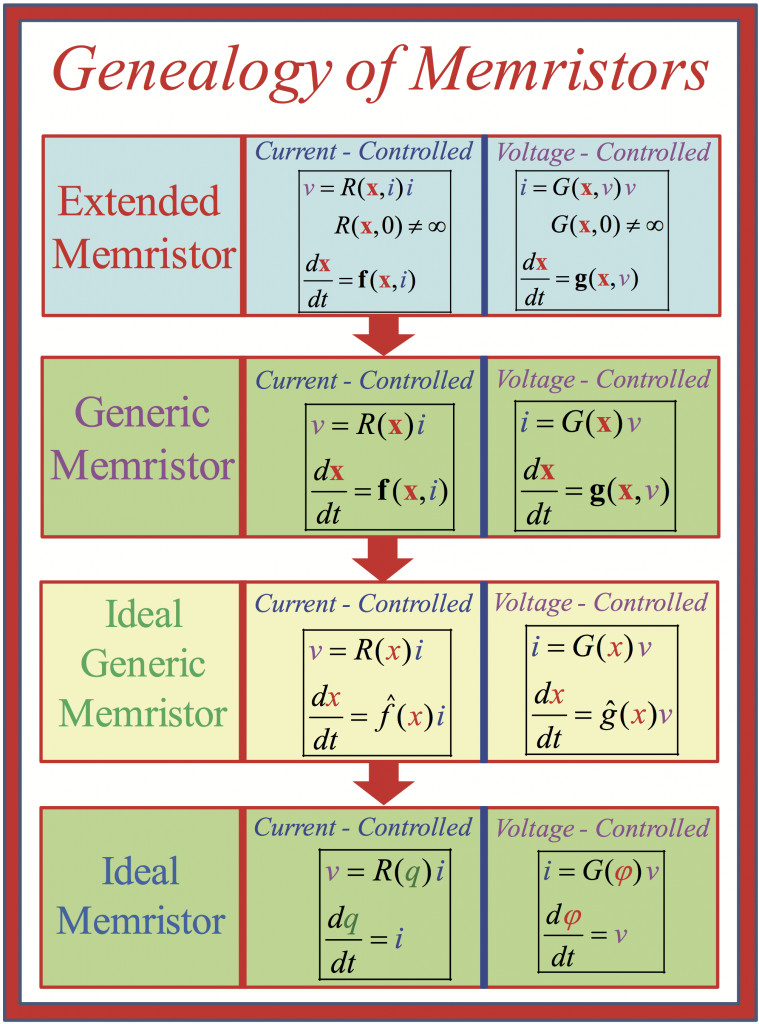
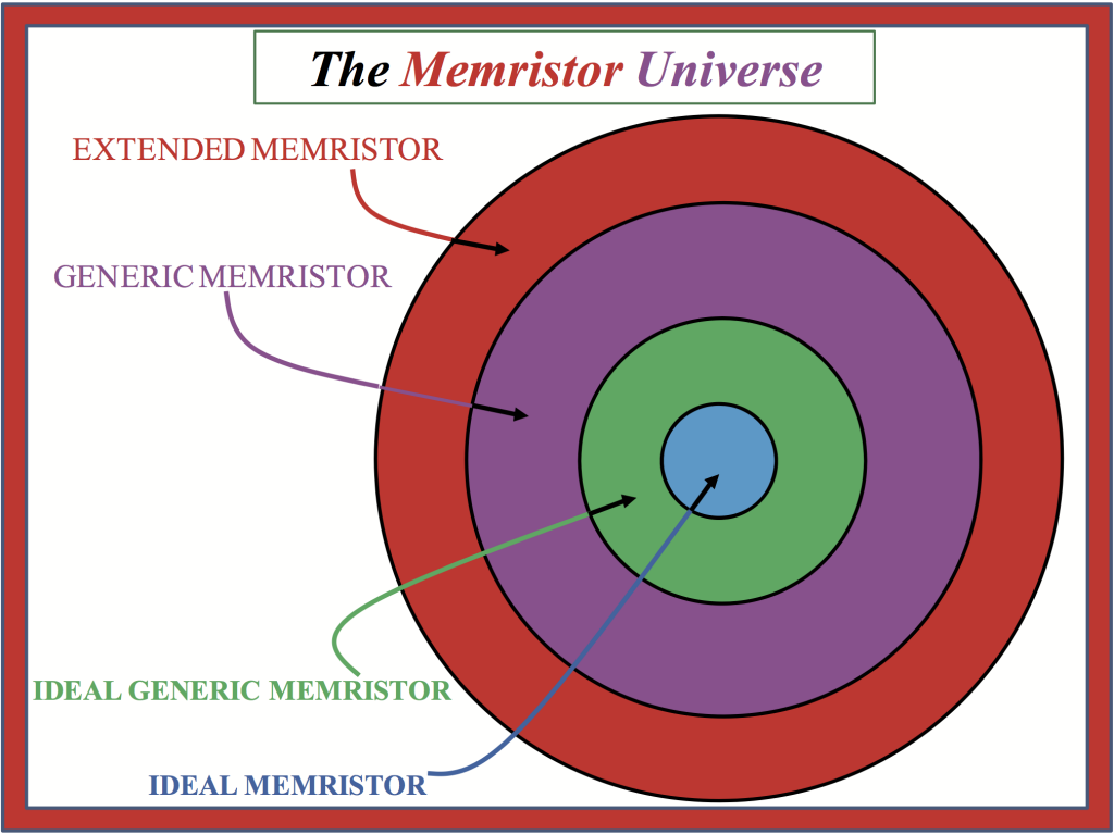
Since then, the interest on memristors and their applications has been growing exponentially, with both academia and industry deploying a huge amount of funds and personnel to fabricate, model, and explore the full potential of these devices in electronics applications. In order to model real-world memristors, L.O. Chua recently generalized the DAE set of ideal memristors (see Figs. 5 and 6 for a complete classification). In the most general class of memristors, referred to as extended memristors, both the state evolution function, i.e. the right hand side of the state ODE, and the memristance (memductance) function in the Ohm law for the current (voltage) input case depend upon state and input. For the sake of completeness, extended memristors had been already proposed but named as memristive systems in a 1976 paper from L.O. Chua and Sung-Mo Kang.
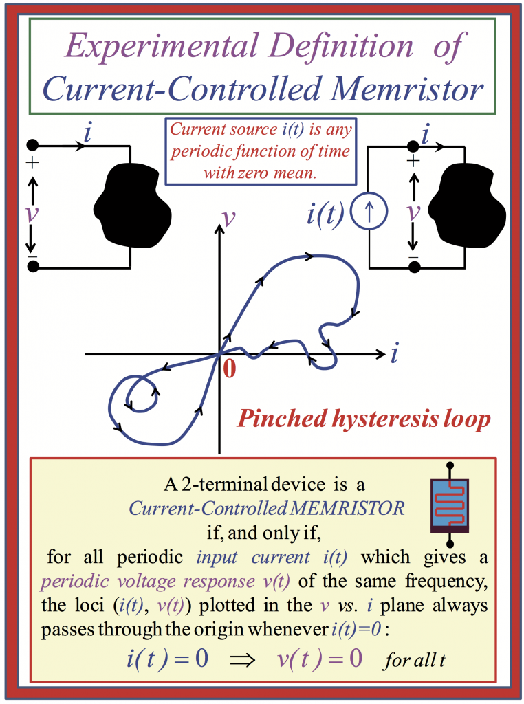
Fig. 3: The pinched hysteresis v-i loop: one of the fingerprints of a current-controlled memristor
Memristor Applications
Real-world memristors promise to revolutionize the world of electronics in the years to come. Importantly, non-volatile memristor nano-devices, capable to retain the information embedded in their states for a practically-infinite time, may allow the design of novel, faster, denser, low power and high-endurance memories. Further, the remarkable similarity between the mechanisms behind the memristance programming of certain physical memristors and the synaptic weight modulation of biological synapses may exploited for the development of novel neuromorphic circuits operating according to biological principles.
However, this is only one side of the fascinating landscape of opportunities real-word memristor nano-devices may pave the way to. Exploiting the complex nonlinear dynamic behaviour of memristors, unconventional data computing paradigms may be implemented in circuit form. This may potentially lead to extend or complement the functionalities of purely-CMOS circuits. To name but one exciting example, some real-world memristors based upon niobium oxide deveopled at Hewlett Packard as well as at NaMLab may amplify infinitesimal signals provided they are biased on the negative differential resistance (NDR) region of their DC current-voltage characteristics. Their use in electronics may pave the way towards the development of novel power-efficient transistor-less circuits for bio-inspired data computing applications, as already demonstrated through the design of a neuristor-based cellular automaton endowed with universal computing capability from R.S. Williams and his research unit.
Fig. 4: A one-dimensional array of 17 memristors based on titanium oxide
Furthermore, the ability of memristors to process signals and store data in the same physical locations may allow the conception of novel mem-computing machines outperforming state-of-the-art hardware systems suffering from the Von Neumann bottleneck, due to the impossibility for the processor to execute a program faster than the maximum rate at which instructions and data may be fetched from and written into the memory. For example, it was recently shown from R. Tetzlaff, A. Ascoli, and D. Ielmini how replacing the resistor of a purely-CMOS circuit implementation of a processing element (PE) of a standard Cellular Nonlinear Network (CNN) with an hafnium oxide-based memristor may allow to shrink considerably the cell IC size. In fact, given that memristor voltages and states are respectively used for data computing and storage, respectively, the inclusion of memory units within each PE becomes unnecessary, allowing to resolve the current mismatch between the densities of light sensor matrices and nonlinear dynamic arrays.
Fig. 5: Memristor classification
Certain memristors may also feature an excellent data sensing capability, which, combined with their miniaturized size, is of great interest in the current Internet-of-Things (IoT) era. For example, it has been shown that ultra-sensitive bio-sensors may be fabricated using these silicon nanowire-based field effect transistors, deprived of the gate terminal. The principle of detection in these innovative sensors is based upon the measurement of the voltage gap opening between the drain current minima in the drain current versus drain-to-source voltage loci in semi-logarithmic scale depending on the concentration of biological analytes bound to bio-receptors previously immobilized on the nanowire-based channel surface.
In view of the promising prospects offered by the introduction of memristors in circuit design, the future will certainly witness the development of novel miniaturized reconfigurable circuits and systems harnessing the memory, processing, and sensing functionalities of resistance switching memories to address open signal processing issues or to determine their solutions in a smarter and faster form and under a lower energy budget expenditure.
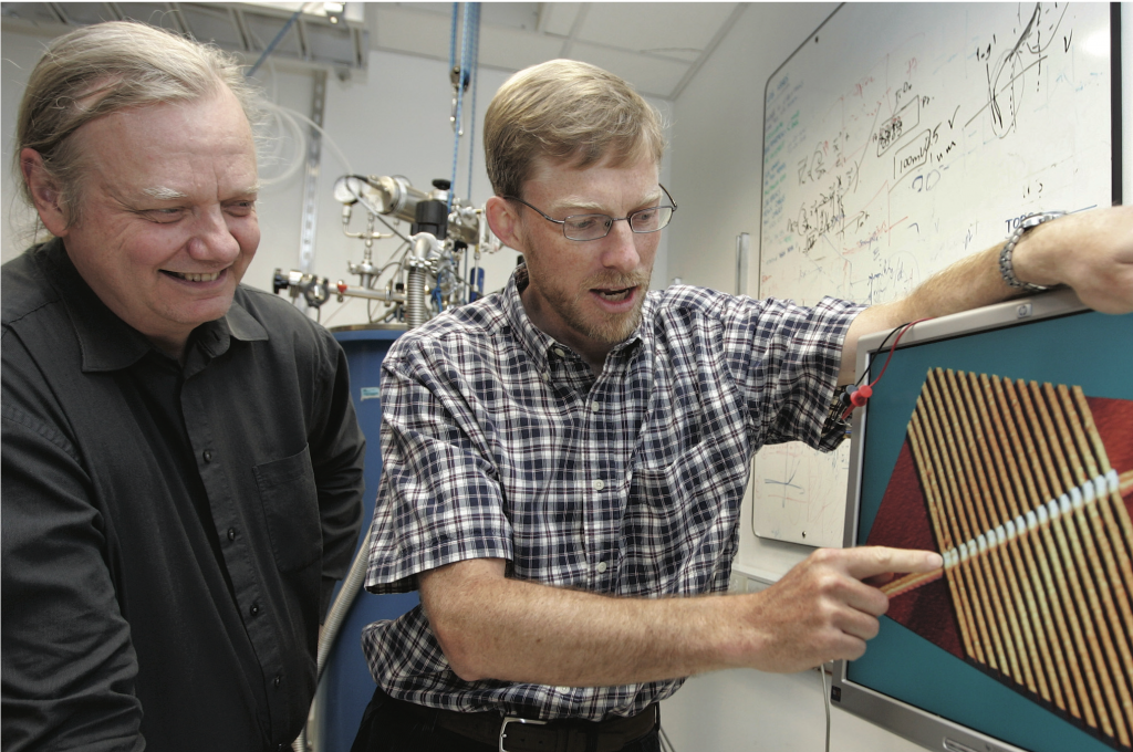
In 2008, the team of R. S. Williams at HP Labs in Palo Alto, CA, built the missing memristor. Watch the story or read the complete article at IEEE Spectrumhere.